How to Use Analog to Digital and Digital to Analog Conversion
download all demo files: AdcDac.7z
1 Analog I/O Pins Usage
Applications of embedded systems are in all domain of life including control and instrumentation system, robotics and electrical appliance. In detecting a physical quantity, sensors play an important role by detecting/measuring a physical quantity such as distance, speed, force, pressure, humidity, light intensity, temperature etc. and then change these properties into the electrical signals which are mostly analog voltage (0-5V) or current (4-20mA).
These physical cannot only be detected by the analog pin of a microcontroller but can also be detected by a digital I/O depending upon the need of application. For example, a photodiode is a device which converts the light energy to current. That current can be fed to analog I/O or digital I/O. If that current is applied to the analog I/O then the I/O pin will read the value between 0-1024 which can be then interpreted between 0-5V by scaling. If the photodiode current is applied to the digital I/O, it will classify it either ‘0’ or ‘1’ based on the threshold defined.
Data received from the sensor or the data which is being processed inside the microcontroller sometime requires the analog to digital conversion or digital to analog conversion. This makes the data fit to become the input or output of certain module. This requires the presence of a module Analog to Digital Convertor (ADC) or Digital to Analog Convertor (DAC) inside the microcontroller. Most of the modern MCUs have these modules and Fio2 STM32F4DISCOVERY is no exception to it.
1.1 Number of Channels
Users can see the number of channels of analog signals from the data sheet of respective microcontroller. Below the figure highlights the pins for ADC to read the voltage from an external device and DAC to send voltage to external devices.
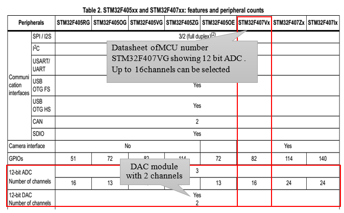
Figure 1‑1: ADC and DAC modules for STM32F4DISCOVERY[1, p. 14]
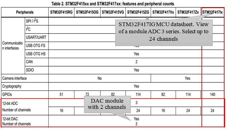
Figure 1‑2: Analog channel modules for FiO2 [2, p. 14]
1.2 Voltage Characteristics
Figure 1‑3 shows the voltage characteristics of ADC. Conversion of voltage range should be between 0V to V REF+ . Power reference voltage should not increase 3.6V and should not be less than 1.8V.
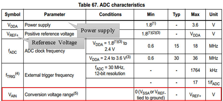
Figure 1‑3: ADC characteristics [1, p. 129]
To read a voltage which is less than 0V (negative) or more than 3.6V, signal conditioning circuit should be used and aMG-SIGCON suits well for this application. Before connecting aMG-SIGCON with the microcontroller [4], it is highly recommended to see the characteristics of aMG-SIGCON from the following website.
http://waijung.aimagin.com/index.htm?amg_sigcon_a.htm
Figure 1‑4 shows the electrical characteristics of DAC module. The maximum output voltage of DAC module is maximum analog supply voltage V DDA – 0.2, where max. V DDA is 3.6V. Operational amplifier is used to reduce the output impedance as shown in [1, p. 137]Figure 1‑5.
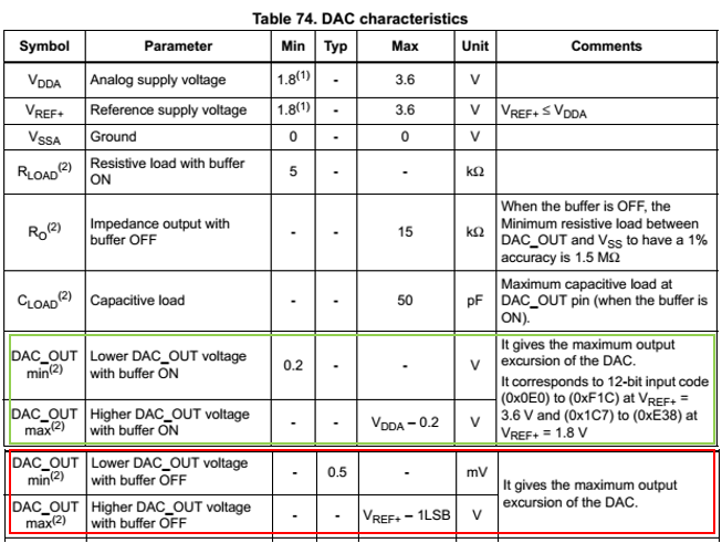
Figure 1‑4: Electrical characteristics of DAC [1, pp. 136-137]
Please note that output of DAC cannot be 0 or exactly V DDA. The buffer gap is about 200mV which is the trade-off for not using operational amplifier.
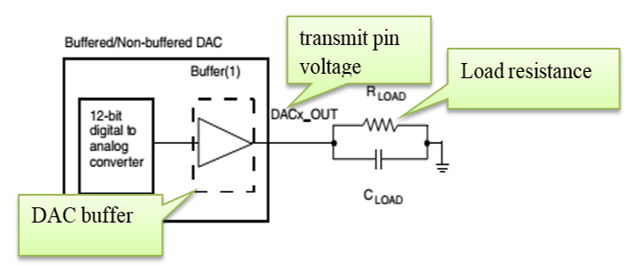
Figure 1‑5: Buffered and non-buffered DAC [1, p. 137]
2 Analog Input Experiments
2.1 How to use Regular ADC Block?
Regular ADC block converts the analog signal into digital data. Users can select the channels and sample rate (sample time) of ADC module for the blockset in Simulink library>>Waijung Blockset>>STM32F4 target>> On Peripheral Chip >>ADC. Regular ADC block has the following characteristics.
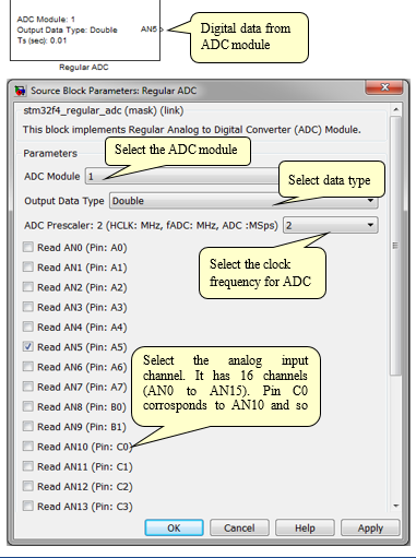
Figure 2‑1: Regular ADC block characteristics
2.2 Experiment to Control LED using Light Sensor
Objective
- To enable the user to read the analog signal using a Regular ADC Blockset
- To understand the fuction of light sensor and enable to the user to control the LED
The sensor aMG Photocell-A is shown in Figure 2‑2. It measures the light intensity. Voltage divider rule can be applied to find the which is governed by the following relationship.
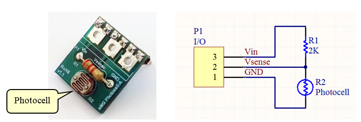
Figure 2‑2: Circuit board for aMG Photocell-A
Table 2‑1:aMG Photocell-A power characteristics
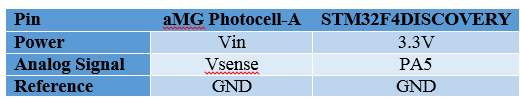
Figure 2‑3 shows a Simulink model for switching the LED. Regular ADC block is used. The working of the model is described as follows;
- The LED will be turned on if the voltage is above or equal to 2.5 V (threshold voltage)
- The LED will be turned off if the voltage is less than 2.5 V (threshold voltage)
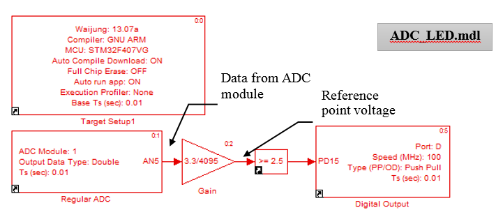
Figure 2‑3: Simulink Model for LED switching using Light sensor
Digital data from ADC module has 12-bit resolution. It is not convenient to display the values from 0 to 4095 on STM32F4. The values from 0 to 4095 does not give us meaningful information therefore it is better to translate this information from 0 to 3.3V with the help of simple transfer fuction (By multiplying with the gain of 3.3/4095.
Figure 2‑4 shows the relationship between the digital values and the actual output. On the x-axis, the digital values are given and on y-axis the corresponding analog voltage value is given.
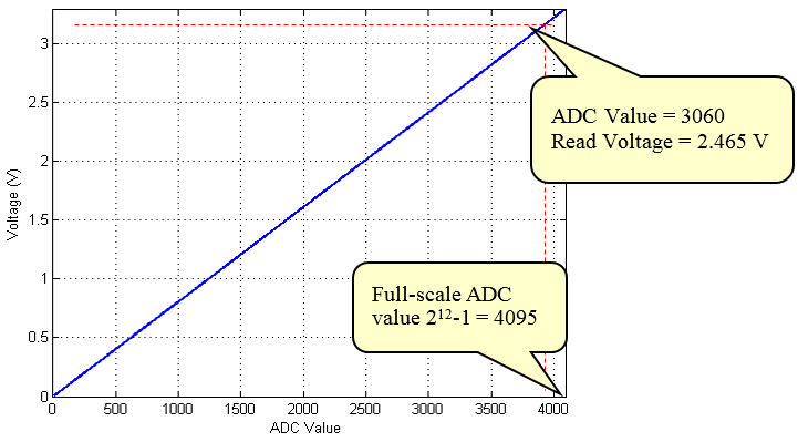
Figure 2‑4: Relationship between digital value and actual voltage
In Figure 2‑4, we can see a red line. For example, the value of ADC is 3060 and we want to obtain its corresponding voltages. To get the corresponding voltages, value of ADC is multiplied by the gain factor i.e.
3060* (3.3/4095) = 2.465V
2.2.1 Using the Display of LCD
The data processed through ADC can be visualized through the LCD panel available on the microcontroller. This can be shown in Figure 2‑5.
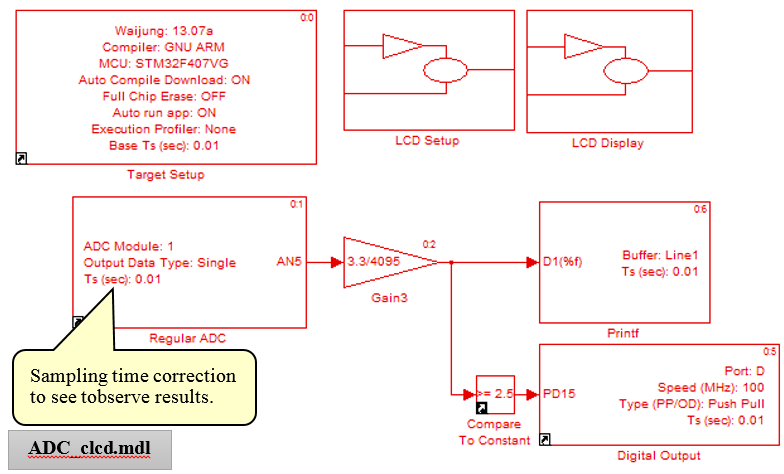
Figure 2‑5: Simulink model for displaying the value of light sensor using LCD display
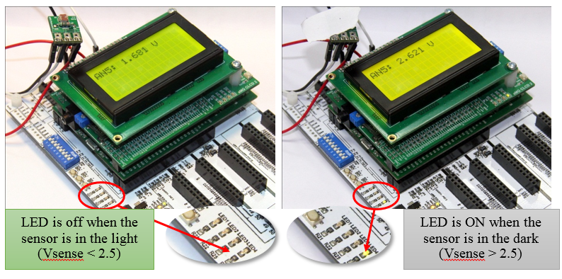
Figure 2‑6: Controlling the LED using light sensor
3 Using the Analog Output
3.1 How to use regular DAC block
Regular DAC block acts via signal DAC1_OUT (pin PA4) or DAC2_OUT pin PA5) for the blockset to control analog output on STM32F4DISCOVERY board. In Simulink library, DAC block can be accessed as Simulink library >>Waijung Blockset >>STM32F4 target >> On Peripheral Chip >> DAC. Regular DAC block has the following features.
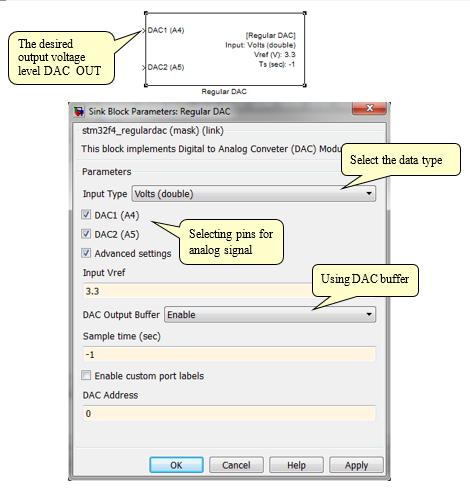
Figure 3‑1: Characteristics and settings of Regular DAC Block
3.2 Experiment to Create a Periodic Signal
Objective
- To be able to create a periodic signal
- To be able to create a periodic signal using Arbitrary Waveform Generator (AWG)
This experiment uses STM32F4DISCOVERY to generate a periodic signal. It has two inputs. The first input is Saw Tooth to pin DAC1 (A4) which has a voltage level between 0V to 1V. The second input is given at pin DAC2 (A5) which has an analog signal frequency of 20 Hz and the voltage level between 0 to 2.5V.
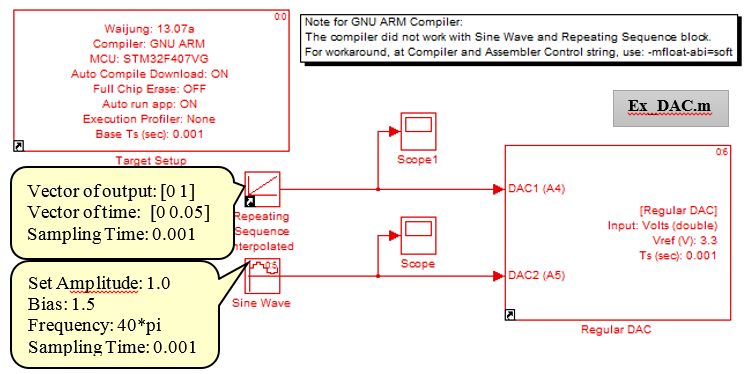
Figure 3‑2: Simulink Model for the Experiment
With the help of the oscilloscope, the signals can be observed. The results are shown below.
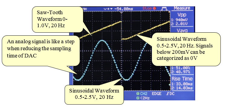
Figure 3‑3: Experiment to generate periodic signal
From the example of Regular DAC Block mentioned above, we use a signal source from Simulink >> Source and its limitation is depended on elapsed time during the trigonometry function calculation. For instance, a sinusoidal waveform of 20 kHz which its period is 50 micro second need to compute the voltage every 5 micro second in order to obtain 10 samples of voltage per pulse and therefore, it may cause the other system not working. Hence, we should use Arbitrary Waveform Generator instead in order to generate high frequency signal that will be discussed later.
3.3 Usability of Arbitrary Waveform Generator
The Arbitrary Waveform Generator developed by Aimagin allows the user to define the dataset. To create a model of the desired signal, the information is downloaded in the memory of STM32F4DISCOVERY. The Arbitrary Waveform Generator has the potential to create a high frequency signal (up to 2MHz frequency from ADC module). Following are the steps to generate a signal from Arbitrary Waveform Generator.
- Define a dataset and enter the command in the Matlab command window.
X = 0:1:49; then press ENTER
Y1 = sin(2 × pi × x/50) + 1.5; then press ENTER
Y2 = 4 × (sin(2 × pi ×x/50) + sin(3 × 2 × pi × x/50) + sin(5 × 2 × pi × x/50)/5)/pi + 1.5; then press ENTER
- The variable x is set to generate a waveform which is from [0, 1, … , 49]. Waveform variable y1 is a signal waveform and y2 is also a waveform with sinusoids. Figure 3‑4 and Figure 3‑5 shows the Simulink model for generating a signal using Arbitrary Waveform Generator and its parameter settings respectively.
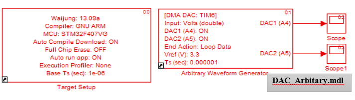
Figure 3‑4: Simulink Model for generating signals using Arbitrary Waveform Generator
- The experiment can simulate the waveform generator to verify the accuracy of the pattern and the frequency of the signal. The word of caution is the signal waveform should be in the range of 0 to VDD (do not forget that there are limits + 200mVfor VDD and 0V with edges.
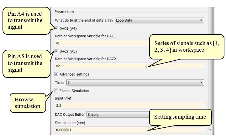
Figure 3‑5: Parameters setting for Arbitrary Waveform Generator
- Download the program and use the oscilloscope signal at pin PA4 (Sinusoidal waveform of 10KHz) and pin PA5 (Square waveform of 10KHz) to the figure below. Please note that the signal is smooth due to higher frequency. The sampling time should be not less than 20 times of the maximum frequency of the signal.
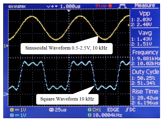
Figure 3‑6: Results generated by high frequency analog signal
4 Miscellaneous Tasks
4.1 Module to Read Analog Value from Digital Signal
Objective
- To test the performance of the ADC module to read analog value from digital signal
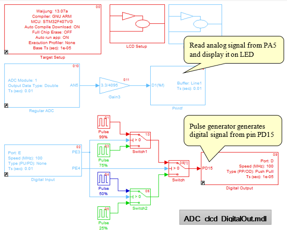
Figure 4‑1: Simuink model to read values from analog signal to digital signals
The Simulink model of this experiment consists of two parts: reading the analog input and displaying the results on LCD screen and creating a digital signal using 4 Pulse Generators with a period of 0.001 second (frequency 1 KHz) each and duty cycle of 25, 50, 75 and 99%.
Digital signal is called Duty Cycle Pulse Width Modulation which is a popular technique for controlling the speed of the motor or adjusting the light bulb. The user can generate the PWM signals using basic PWM or Advanced PWM blocks in Simulink library >> Waijung Blockset >> STM32F4 target >> On peripheral Chip >> TIM.
After downloading the program to STM32F4DISCOVERY, pin D15 will send a digital signal with a frequency of 1 KHz. User can select the duty cycle of the digital signal by setting DIP switch as shown in Table 4‑1. Pin D15 is to be connected with an RC circuit which serves as a first order filter for the signal as shown in Figure 4‑2. Signal after filtration will be sent to the LCD for display.
Table 4‑1: DIP switch for changing the duty cycle
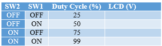
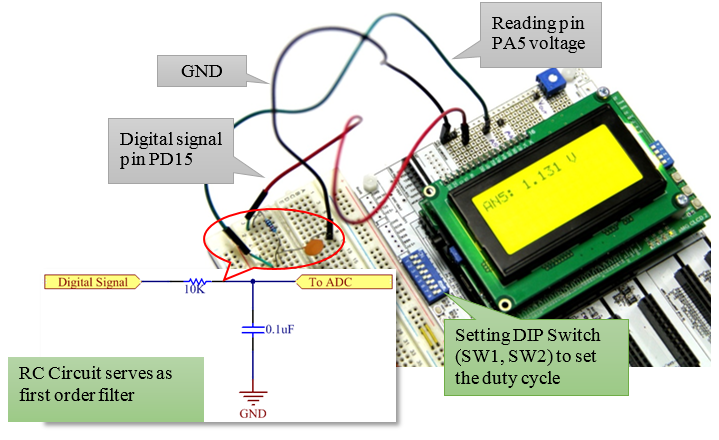
Figure 4‑2: Reading Analog Value from Digital Signal
Values of the RC circuit will vary depending on the selection of the duty cycle. For this experiment, the values are taken to be R = 10 Kohm and C = 0.1uF.
4.2 Digital Input Analog Voltage Reading
Purpose
- To understand the functionality of analog signals to Digital Input
- To study the divided state of Digital I/O with input voltages of STM32F4
In this experiment, potentiometer (variable resistor) is used for analog signals. Pin PA5 is configured so that it received analog signals and pin D15 is configured to have a digital input form. Figure 4‑3 shows in the Simulink model which includes the LCD setup and LCD display. PD14 is the digital output which is connected to LED3 which can be act according to the signals on PD14.
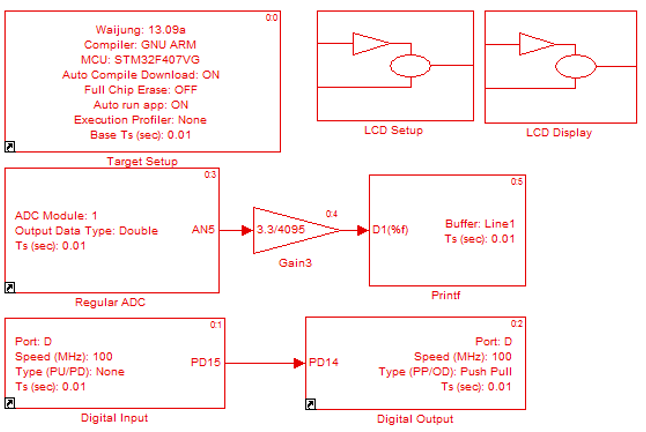
Figure 4‑3: Simulink model for analog signals to digital input
After downloading the program on STM32F4 DISCOVERY, the voltage of the potentiometer can be observed on the display LCD. The blinking of LED3 and LED4 is controlled by the following table.
Table 4‑2: Results
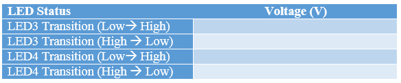
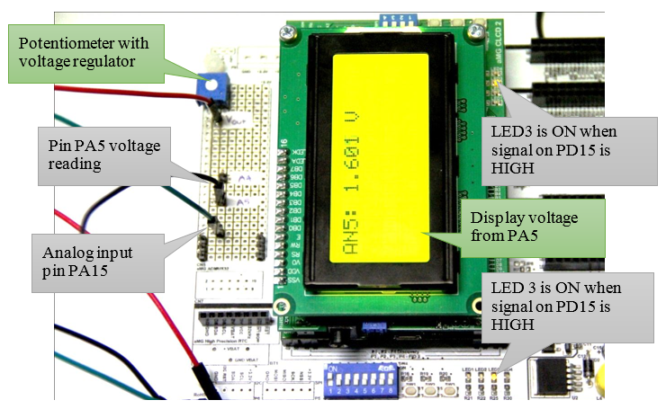
Figure 4‑4: Reading digital input signal
4.3 Selection of Sampling Rate
To convert an analog signal to digital one, sampling time plays a crucial rule. Sampling time determines at which time the sample should be taken. For example, if sampling time is set to be 0.01 sec, this means that the signal is measured and converted the analog to digital signal after every 0.01 second i.e. 100 Hz (Sampling frequency).
Choosing an appropriate sampling rate is very important. If the sampling rate is very less then error introduced in the system will be more. If the sampling rate is very high, then it requires high computation power and memory [7]. In order to have an appropriate sampling rate, Nyquist criteria determines the frequency. According to the Nyquist theorem, the sampling frequency should be twice the frequency of the signal. If there are multiple frequencies in the signal then sampling frequency should be twice to the maximum frequency of the signal [8].
One thing should be remembered that the sampling frequency also depends on the requirement of the application. If the bandwidth requirements are not strict then there is no harm to exceed Nyquist sampling frequency. Nyquist theorem only tells the minimum requirement of the sampling frequency. If the sampling frequency is below Nyquist theorem, then signal cannot be reconstructed. In some applications, the sampling frequency is taken to be 20 times the maximum frequency of the signal to be very close to the original signal.
In this experiment, the sampling time of ADC module is taken to be 0.01 second (which can be changed to desired value) and this sampling time is used to read the analog sinusoidal waveform with different frequencies of 5Hz, 20Hz, 50Hz and 60Hz (User can use Function Generator to create the above mentioned frequencies instead of using Regular DAC block y setting the minimum and maximum voltage of 0.5 – 2.5V). Following are the steps to accomplish this experiment.
- Pin PA4 is connected to pin PC0 and aMG USB Converter-N Adapter (for details click here) to board aMG F4 Connect 4 in Figure 4‑5
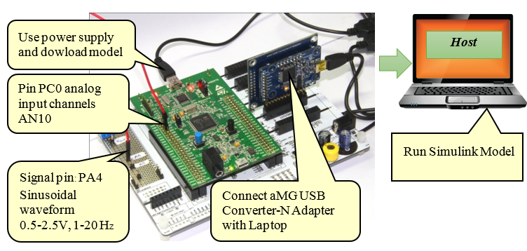
Figure 4‑5: Analog to Digital Conversation
- Download Simulink model in Figure 4‑7 into STM32F4 DISCOVERY. Pin PA4 voltage is applied to PC0 to read sinusoidal waveform. The digital signal is sent via USB cable to the PC/host
- Host need to open Simulink model and set the configuration as per Figure 4‑6 (Host Serial details can be found from here)
- After clicking on Run Simulation, user can select the frequencies by using Dip Switch SW1 and SW2 and observe the signal on the scope. The experimental results are shown in Figure 4‑8
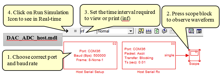
Figure 4‑6: Simulink model for reading voltage
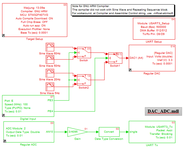
Figure 4‑7: Sample rate selection for Simulink model
Table 4‑3: Sample rate selection for the host
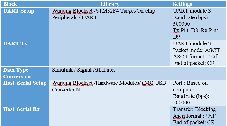
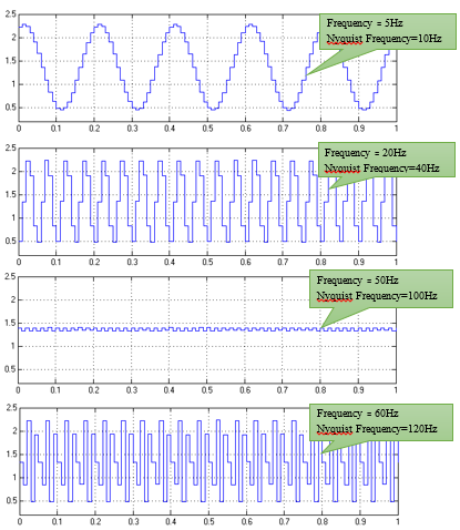
Figure 4‑8: Waveforms of 5, 20, 40, 50 and 60 Hz with sampling frequency of 100 Hz
The above figure shows the waveforms for different frequencies from 5 Hz to 60 Hz. The sampling rate for all the waveforms is set to be 100 Hz. From the Nyquist criteria, it is known that for 60 Hz waveform, 100 Hz sampling frequency is not high enough to reconstruct the signal. For practical purpose, the sampling frequencies are taken to be 20 times more than the maximum frequency of the signal.
5 References
- STMicroelectronics, STM32 F407xx Datasheet-production data [Online], 2013
- STMicroelectronics, STM32 F417xx Product-Specification [Online], 2013
- STMicroelectronic, UM1472: STM32F4DISCOVERY User Manual [Online], 2012 .
- Aimagin, Signal Conditioning Design Guideline, [Online]. Available: http://waijung.aimagin.com/signal_conditioning_design_gui.htm.
- Aimagin, aMG Photocell – A, [Online]. Available: https://www.aimagin.com/amg-photocell-a.html
- E. W. Weisstein, “Fourier Series. From MathWorld–A Wolfram Web Resource.,” [Online]. Available: http://mathworld.wolfram.com/FourierSeries.html.
- R. G. Lyons, Understanding Digital Signal Processing, New Jercy: Prentice Hall PTR, 2001
- S. J. Orfanidis, Introduction to Signal Processing [Online]. Available: www.ece.rutgers.edu/~orfanidi/intro2sp, 2010.
- STMicroelectronics, RM0090: STM32F40xxx Reference Manual [Online], 2013