How to Use Digital Input Output
Download all demo files: DigitIO.7z
1 Digital Input / Output
Typical applicatons of microcontroller involves the tranfer of data to and from the MCU to external device. Figure 1‑1 shows a microcontroller which can be used for transfer of information. Data transfer can be achieved by utilizing input and output pins (I/O pins). Input pins are responsible for receiving the information from the external devices which is then sent to the memory for storage or/and processing. Output pins are responsible for sending information to the external devices. This information may come either from the memory or by processing the information within MCU.
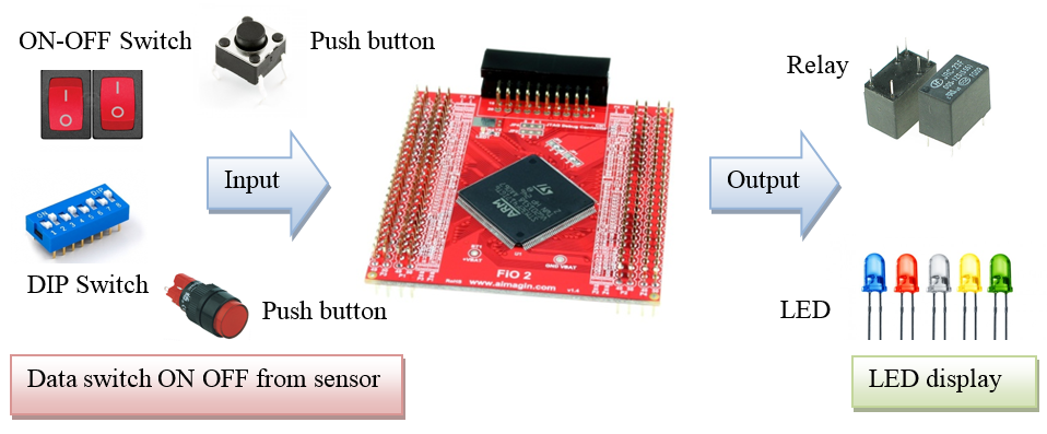
Figure 1‑1: Transmission and reception of data between microcontroller and external device
Digital I/O is a form of a signal which only have two states or logic levels.
- Logic LOW corrosponds to 0
- Logic HIGH corrosponds to 1 or a non-zero state
So basically Digital I/O transfer/receive data to/from an external device which is binary in nature. Digital output is used to control devices such as frame relay or LED lamps that requires only turn on and off signals. Digital input is used to read data from a device such as switch or button that is turned on and off. (In contrast there is also an Analog I/O).
Now the question comes, how we can classify logic level low and logic level high? The answer to this queston is very simple. In electronics, if the voltage level is above certain level, it is classified as low and if is below certain level, it is classified as low. Figure 1‑2 shows the digital logic levels for STM32F4 (STMicroelectronics, DS8626: STM32 F407xx Datasheet-production data [Online], 2013, p. 110).
When using the Transistor Transistor Logic (TTL)
- When the voltage level is below 0.8V it is considered as LOW
- When the voltage level is above 2.0V it is considered as HIGH
When using the CMOS technology, logic LOW and HIGH are determined based on power supply voltage V DD. For example when V DD = 3.3V
- LOW state is when the voltage is below 0.99V (0.3×3.3)
- HIGH state is when the voltage is above 2.31V (0.7×3.3)
For determining the logic levels of a microcontroller, datasheet must be referred.
Hysteresis refers to the difference in the voltage levels between the detection of the transistion level from high to low and vice versa. Hysteresis is very useful technique to overcome the issue of noise. If we define a simple criteria that above 0.5V is high and below 0.5 is low then becuase of noise effect, a 0.49V signal can go to 0.51V thus logic is inverted from the original. Hysteresis gives protection and robustness against such surges. Compared with TTL technology, it gives a range of voltages to be LOW or HIGH.
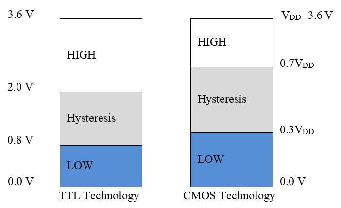
Figure 1‑2: Digital logic levels for STM32F407xx
1.1 Input Circuit
Each pin of STM32F4 can be characterized as one of the three types i.e. Pull-Up, Pull-Down and Floating (In addition, some pins are particularly 5V Tolerance. Users need to refer to the datasheet of specific MCU to see if it is 5V tolerance).
1.1.1 Pull-Up Circuit
Figure 1‑3 shows a pull-up input which is basically is a pull-up resistor connected to VDD or power supply. Pull-up circuit serves the purpose of reading the status automatically in the microcontroller. If pull-down is disconnected then the state is HIGH i.e. “1” all time and if it is connected then the state is LOW i.e. “0” (Active Low). When the switch is pressed then MCU pin goes LOW. Circuit pull-up is better as compared to circuit pull-down as former is more robust to noise.
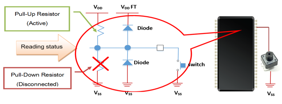
Figure 1‑3: Pull-up circuit
1.1.2 Pull-Down Input Circuit
Figure 1‑4 shows the condition when the pull-up resistor is disconnected from VDD and pull-down resistor is connected to the ground while reading the automatic status from MCU. For the given condition, the circuit will read LOW i.e. “0” all the times and when the switch is pressed it will start reading HIGH “1”.
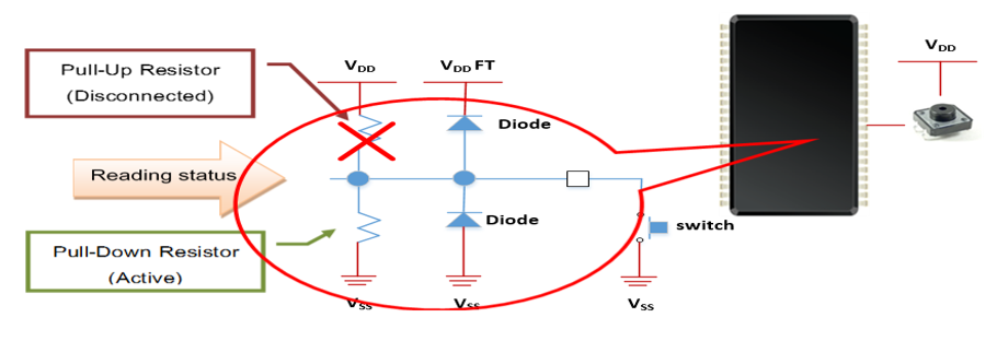
Figure 1‑4: Pull-down input circuit
1.1.3 Floating Input Circuit
Setting pin value to floating has the same idea as pull-up / pull –down but no internal pull-up and pull-down resisters is required. User must connect the pull-up or pull-down externally so it is suitable for some device that already has external Pull-Up or Pull-Down.
1.2 Output Circuit
The output of STM32F4 are of two types i.e. Push-Pull or Open-Drain. User can choice either of them.
1.2.1 Push-Pull Output Circuit
STM32F4 can be set as a Push-Pull output. Internal circuit of microcontroller has two types of MOSFET: the P-MOS that connected between V DD and output pin for transferring current (Source Current) and N-MOS that is connected between output and ground for receiving current (Sink Current). This is shown inFigure 1‑5. The automatic connection control can described below:
- When needing output status HIGH/“1” system will open P-MOS and close N-MOS, then the output will have voltage = V DD /“HIGH” state.
- When needing output status LOW/“0” system will open N-MOS and close P-MOS, then the output will have voltage = Ground/“LOW” state.
From Figure 1‑5, we can see that when connecting a LED between output pin and ground, a resister is used to limit the current. LED will work when output state is “1” (Active High Output). Because of the output has voltage level VDD so the current can flow from microcontroller through LED to the Ground.
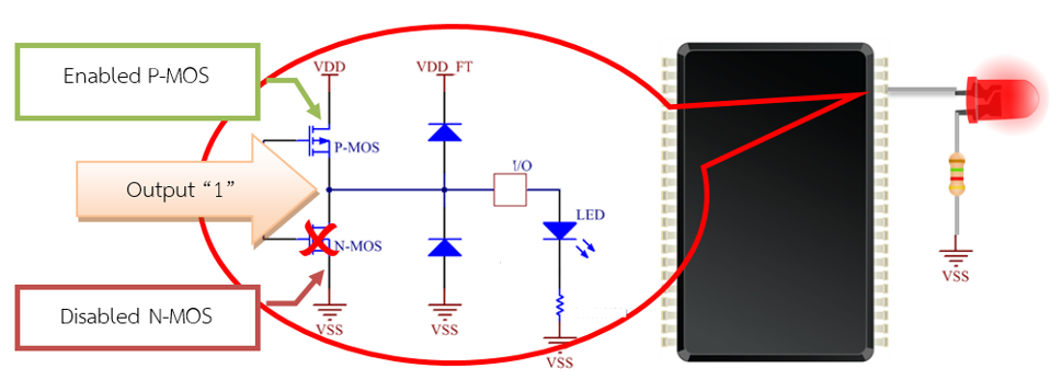
Figure 1‑5: Push-Pull output circuit current for sourcing system
When connecting a LED between output pin and external V DD, resister is used for limiting the current as see in Figure 1‑6. LED will work when output state is “0” (Active Low Output) because the current can flow from V DD through LED to output pin (Ground)
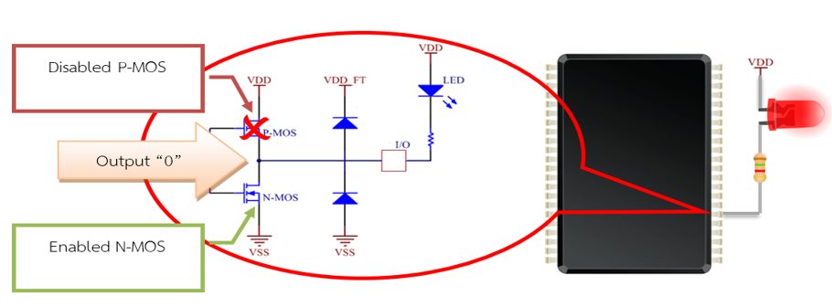
Figure 1‑6: Push-Pull output circuit current for sourcing system
The advantage of Push-Pull output is that it can quickly change its state, so it is suitable for such a situation which requires high frequency switching (e.g. visible light communication [4]) and it can directly transfer current to device. The disadvantage of this type is the limitation of current source/sink. User must study pin’s maximum current and voltage values from datasheet of each microcontroller. These information are very important to prevent device from damage and to improve the system reliability. For example, each pin of STM32F4 can sink/source maximum current at 25 mA except PC13 – PC15 can sink at 3 mA [1, p.77] and can sink/source maximum of all pins not more than 150mA as shown in Fig 2-7. Thus when bias the LED with Push-Pull I/O (assume that VDD = 3.3 V) we can use R = 660 Ohm (from R = V/I = 3.3/5m = 660) to limit current at 5mA that enough to make the LED bright and not exceed the 25mA maximum value.
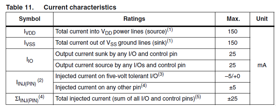
Figure 1‑7: STM32F415xx-417xx Absolute maximum ratings: Current characteristics [2, p. 73]
1.2.2 Open-Drain Output Circuit
When setting the output of STM32F4 to Open-Drain, internal circuit in each pin of microcontroller will be controlled automatically as below:
- Output register will close P-MOS in any state
- If output state LOW or “0” is needed, system will open N-MOS, then output pin will has same voltage as ground.
- If output state High or “1” is needed the system will close N-MOS then output will be High Impedance state.
So the Open-Drain output must connect to external electric source Vext as shown in Figure 1‑8 that the device will work at output state “0”
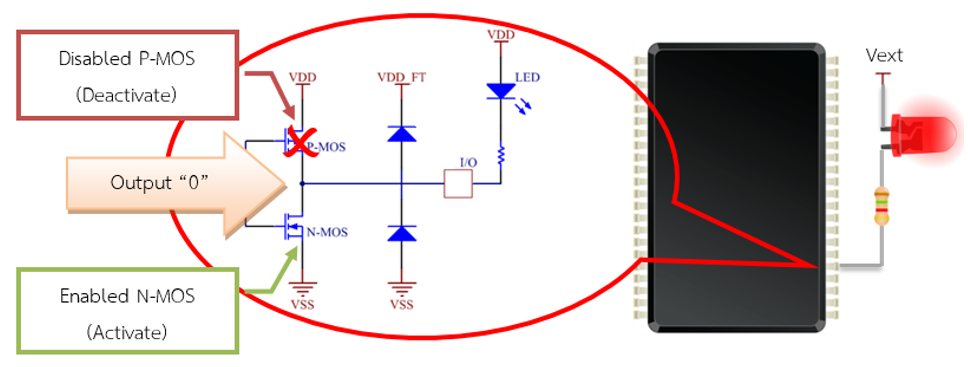
Figure 1‑8: Open-Drain output circuit
Since the Open-Drain circuit doesn’t use power from microcontroller, it can be advantageous because devices are using external power which can have a voltage might be higher than V DD. However user must be careful about maximum current must not exceed 25mA. Furthermore this type is suitable with bus system such as I2C too.
2 Digital I/O Experiment
2.1 Experimental Devices
Experiment of digital I/O uses basic devices such as LED to display digital output state, switch button (ON-OFF), and dip switch to create logic of input signal to digital input. These devices (LED etc.) can be easily purchased and they are not expensive.
The board aMGF4 Connect2 developed by Aimagin can be used with STM32F4DISCOVERY. FiO2 has 4 LEDs, 3 ON-OFF swithes and 8-pin dip switch as shown in Figure 2‑1.
The board STM32F4DISCOVERY developed by STMicroelectronics uses microcontroller series. STM32F4 number STM32F407V6T6 has 100 pins and able to use digital I/O maximum at 82 pins. It has 6 ports: PA, PB, PC, PD, PE and PH, having 16 pins in each port (except PH, has 2 pins) each pin can be set as output or input. For example, we can set PD1 to be pull-up input and PD7 to be push-pull output (details can be found in the microcontroller datasheet about each pin). The board FiO2 uses the microcontroller number STM32F417IG that has many more pins but the principle is the same.
Be careful that when using STM32F4DISCOVERY, some pins may be already connected with other device on the board so we have to study the datasheet wisely.
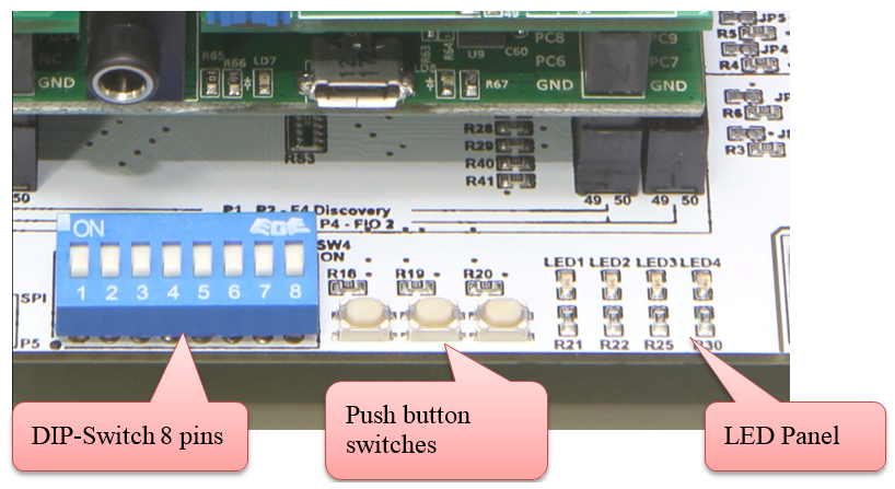
Figure 2‑1: Tool on aMG F4 Connect 2 for testing Digital I/O
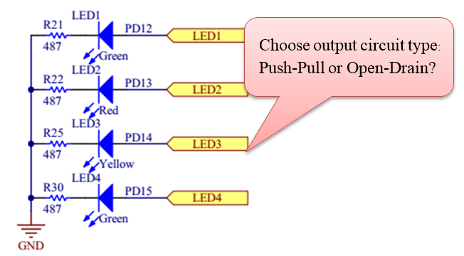
Figure 2‑2: LED circuit on aMG F4 connect board
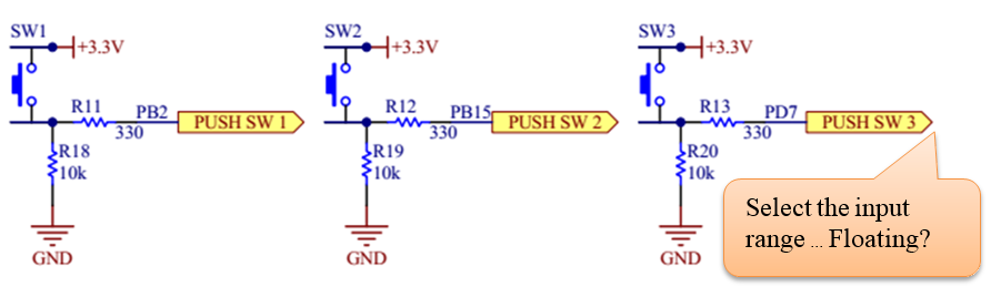
Figure 2‑3: Push/Pull switching circuit on aMG F4 connect board
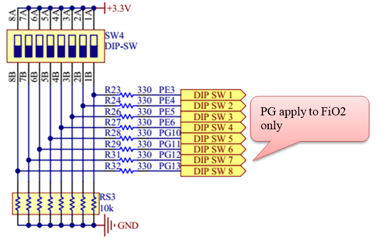
Figure 2‑4: DIP switching circuit on aMG F4 connect board
2.2 How to Use Digital Output Blockset
The blockset used to control digital I/O is in STM32F4DISCOVERY can be found from Simulink library >> Waijung Blockset >> STM32F4 target >> On Peripheral Chip >> I/O by Digital Output block. It has the following characteristics as shown in Figure 2‑5.
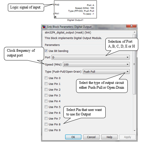
Figure 2‑5: Characteristics and settings of digitial output block
2.3 Blinking LED
Purpose
- Enable the users to simulate the real enviornment before they actual implement.
- Enable the users to control the switching of LED by using Pulse Generator block which determines the switching speed
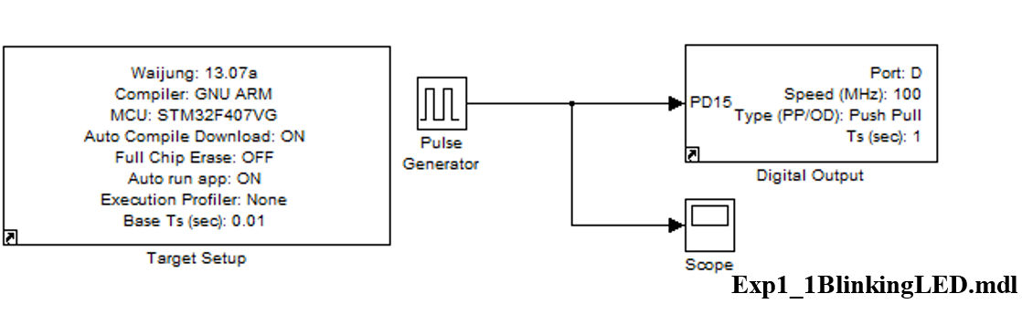
Figure 2‑6: Simulink Model – Testing the blinking of LED 1
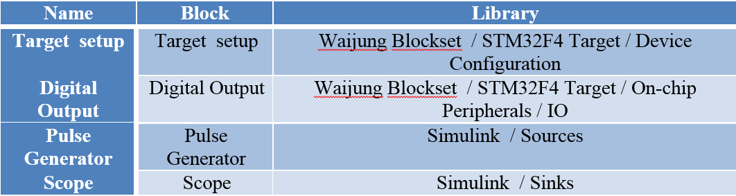
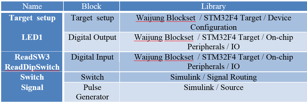
Table 2‑1: Simulink blocks used in blinking LED experiment
In setting parameters of Pulse Generator Block there is an important parameter called Period or the period of waveform. Pulse width gives the information that for how long the LED will be in ON state and for how long it will be in OFF state for a given time. For example, user wants to switch on the LED for 1 sec and switch off the LED for 3 sec and this process keeps on going. For the given case, the pulse width can be calculated by using relation below.
% Pulse Width = (Time for which LED is ON) x 100 / Period
Here Period corresponds to switch ON + switch OFF time i.e. 1 + 3 = 4 sec. So the answer is:
= (1) x 100 / 4 = 25 %
We can simulate the Pulse Generator Block as shown inFigure 2‑8. Pulse type is selected as time based, amplitude is choosen to be 1, period is taken to be 4 sec with 25% pulse width. Click on start simulation by clicking on the Run Icon as shown inFigure 2‑7. Double click on the Scope to see the simulated waveform as shown inFigure 2‑8. The user will not be able to see any LED blinking apparently. But the user must think in mind what does this waveform mean and how to interperet this waveform in terms of hardware? The positive pulse means that the connected LED (right now in simulation not connected) will be ON and when there is no pulse then the LED will be OFF. Furthermore user can observe that for 1 cycle, the LED will be ON 25% of the time and will be OFF for 75% of the time.
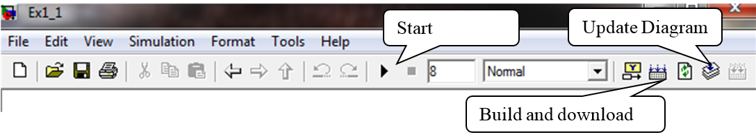
Figure 2‑7: Understanding three icons of Simulink
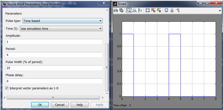
Figure 2‑8:Setting the Pulse Generator Block and blinking LED experiment results
When the user is satisfied that in simulation, the program is working well then the next step is to download the program in the target. Downloading of the program to the target can be done either by pressing CTRL+D or by clicking the icon Update Diagram and then pressing CTRL+B or clicking icon Build and Download as shown inFigure 2‑7. If the downloading of the program is successful to the target then LED6 of STM32F4DISCOVERY and LED4 of aMG F4 will be switched ON for 1 sec and switched OFF for 3 sec and this process keep on repeating. Now it is left on the user to do some experimentation by changing the amplitude, period and pulse width and see the effect on the simulated waveform and verify the similar effect on target LED.
2.4 Running LEDs
Purpose
- Enable the users to use Pulse Generator for periodic signal creation
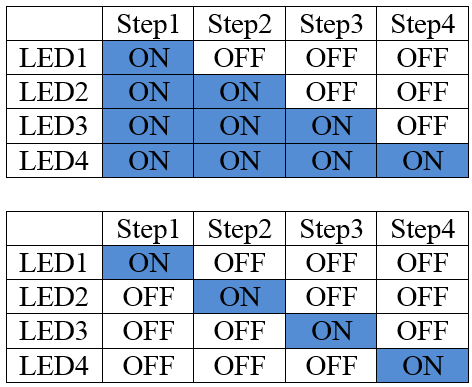
- Enable the users to control the switching of 4 LEDs simultanuously. The four LEDs should follow the pattern as shown in the table below.
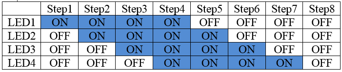
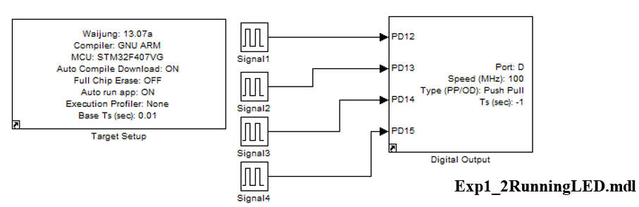
Figure 2‑9: Simulink Model – Controlling 4 LEDs simultaneously
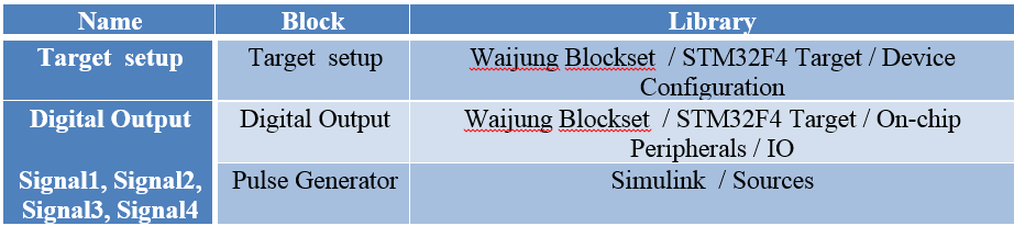
Table 2‑2: Simulink block required resources
In this simulation, four LEDs are used. These LEDs are switched ON and OFF in a pre-determined manner as given in the table. Let’s assume that we need to complete 8 steps in 2 seconds. It means that each step is for 0.25 sec. When 8 steps are completed, the system will again go to step 1 and this process keeps on happening. If the user observes the steps table carefully thenuser can know that each LED is ON for 0.25 × 4 = 1 sec and for the same time it is OFF. This implies that the pulse width of all LEDs is 50%. Pulse Generator Block has a period 2 sec.
Another information which can be extraced from the table is in the first step only LED1 is on. In second step LED 1 and LED 2 is ON. In third step LED 1, 2 and 3 is ON and in fourth step all LEDs are ON. This means that there is some time delay between these LEDs. Time delay of LED 2 is more than LED1. Time delay of LED 3 is more than LED1 and 2. Time delay of LED4 is more than LED 1, 2 and 3. We can also write that:
- Time Delay of LED 2 with respect to LED1 = 0.25×1 = 0.25 sec
- Time Delay of LED 3 with respect to LED1 = 0.25×2 = 0. 5 sec
- Time Delay of LED 4 with respect to LED1 = 0.25×3 = 0.75 sec
For this example, block from Simulink Source Library such as Counter Free Running Block or Pulse Generator Block will be used as controlling signal for open-close output. When external signal is needed (for example: switch) user can use Digital Input Block to receive signal that is in Simulink Library >> STM32F4 target >> On Peripheral Chip >> I/O.
2.5 How to Use Digital Input Blockset
For Blockset controlling Digital I/O of STM32F4DISCOVERY board, go to Simulink Library >> Waijung Blockset >> STM32F4 target >> On Peripheral Chip >> I/O. Digital Input block and it has the following characteristics.
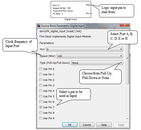
Figure 2‑10: Settings of digital input block
Further more users can define a sampling time and enable custom port labels to name the input port according to their wish.
2.6 Controlling LED from Push Button
Purpose
- Enable the users to read values by programming the push buttons using Digital Input Block
- Enable the users to understand the working of Jog and apply it to real environment
- Enable user to read the value from push button and Toggle the Output
- Enable users to compare the performance of Toggle and Jog
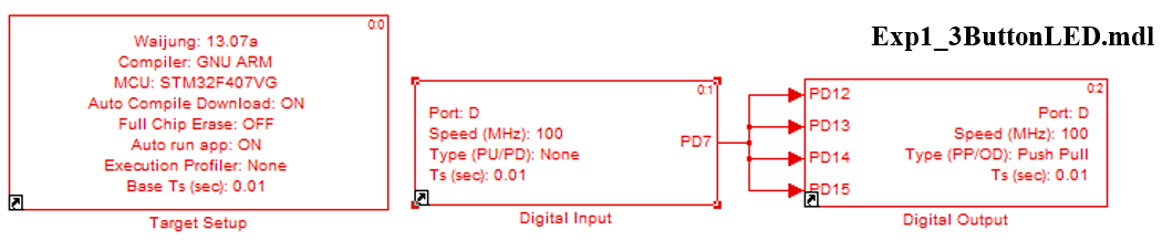
Figure 2‑11: Simulink model ON OFF switching of LED with push button
Table 2‑3: Simulink block for contolling LED switching using push button
When user has downloaded model into STM32F4DISCOVERY, 4 LEDs will ON when pressing the SW3 and OFF SW3 is not pressed. So the Jog is programmed so that it always send output when the button is pushed and stop sending when button is not pressed. This scheme is suitable for control manual machine such as crane or lifting machine.
2.6.1 What is Bouncing/De-bouncing?
Bouncing is the non-ideal behavior of mechanical switches which creates multiple electric transitions when a single input from the user is entered. It takes some time for the input to reach at a stable state. The bouncing effect is shown inFigure 2‑12. From the figure, we can see that in the begninning the switch is in ON state. When user enter the input to switch it OFF, then it takes around 0.01 to 100 msec before the switch is actually switched OFF. A similar effect can be observed when the switch goes from OFF state to ON state.
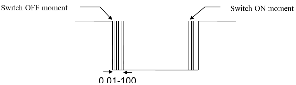
Figure 2‑12: Bouncing effect
Bouncing is an undesirable effect so it must be removed when designing a circuit. There are number of ways by which we can avoid bouncing. The process of avioding bouncing is called de-bouncing. The most easy and commonly used technique for debouncing is analog filtering. A resistor capacitor (RC) circuit is used to filterout the rapid changes in the switch output. Depending on the nature of the switch, the values of RC circuit is chosen in such a way that input threshold is not crossed while bouncing is still occuring.
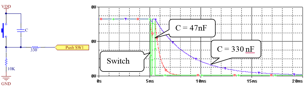
Figure 2‑13: RC circuit for debouncing
Other than hardware techniques available to overcome debouncing, software programming can also help to aviod it. This will eliminate the need to additional RC circuit. In RC block, the user can also set the time interval in Waijung Blockset have Debounce block in Simulink Library: Waijung Blockset >> STM32F4 Target >> On-chip Peripherals >> IO by setting parameter of Debounce block.
Mode can be selected as Normal, Single End and Toggle Latch. The user can change working mode and observe the behavior of LED when pushing the button and debounce counting. Toggle mode is the program to always send output when push the button at a time, and stop sending when pushes it again. Thus the program should check the status of output, and send new status of output when the button is pushed. The Toggle is suitable for on-off electrical device.
Debouncing block can be added in between digital input and digital output as shown in Figure 2‑14.
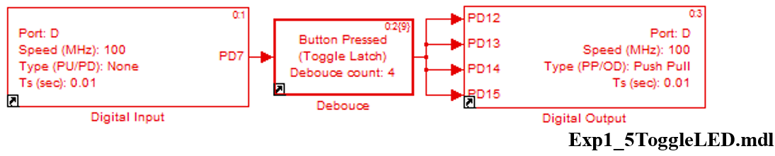
Figure 2‑14: Simulink model for LED control using push button (Toggle mode)
2.6.2 Self Practice Exercise
- Explain the difference in LED switching when using the following modes : Normal, Single End and Toggle Latch
- Explain: on-off of LED when increase Debounce Count in Normal mode
2.7 Experiment to switch LED via Dip Switch
Purpose
- Enable the user to read value from dip switch
- Enable the user to control the switching of LED while operating via dip switch
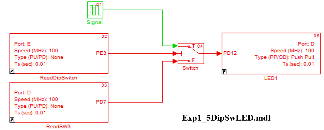
Figure 2‑15: Simulink Model to switch LED via dip switch
Table 2‑4: Simulink block used to control switching of LED from DipSwitch
In this experiment, switching of the LED is controlle via dip switch1. Pin PE3 is connected to switch block which will be selected according to the conditions. (This is true when input signal is not equal to 0) Figure 2‑15 shows when condition is true, signal from Pulse Generator is used to control switching of LED.
When dip switch is ON then LED will blink for every 0.5 second and when the dip switch is OFF then LED will be ON when SW3 switch is pressed. This task can be achieved with multiple mode of operations such as automatic mode or manual mode.
3 Digital I/O
Purpose
Design a program such that it switches ON one LED in each round from the four LEDs using counter and bit operation (Be able to look Model from digital output demo stm32f4_digital_output_demo.mdl)
Explanation
- Setting the parameters of the counter;
- Set number of bits (n) equals to 16;
- Sampling time: 0.5.
When the program starts running, the counter is reset after every 500 msec. Counter starts counting from 0 to 2n-1 which is the highest number in counting. It will again count from 0 and the counter will AND it’s output with constant 3 so that the counter value is in interval 0 to 3 only. After that, it uses block compare to constant to assign the switch ON the LED1, LED2, LED3, LED4 when the value of the counter is 0, 1, 2 and 3 respectively.
The following table explains the working of the program. Each step is for 0.5 seconds. When the step 2 is completed, the program is returned to step 1.
Design a driver for LED 4 working as follows.
4 Frequently Asked Questions (FAQs)
Question: STM32F4DISCOVERY and FiO2 are with how many I/O pins?
Answer: STM32F4DISCOVERY that use microcontrolller STM32F407VGT6 or use FiO2 that use microcontroller STM32F417IGT6, users can see the information from Datasheet Product Specification. For example the number of GPIO or (I/O pin) of STM32F407Vx is 82 (STMicroelectronics, DS8626: STM32 F407xx Datasheet-production data [Online], 2013, p. 14) STM32F417Ix has 140 pins [2, p. 14]

Figure 4‑1: Shows the number of I/O pins of all STM32F40xxx models
Question: Which I/O pin to be used?
Answer: User should find the type and characteristics of I/O pins from datasheet.
- Digital I/O can have a voltage of 5.0V (5V tolerance I/O). Resistor (R) should have respective value to avoid crossing maximum applied voltage;
- For analog pin, donot apply more than 3.3 V;
- Out put voltage is between 1.8 V to 3.6 V.
Question: What I/O pins can supply?
Answer: Voltage up to 3.6 V and current not exceeding 25 mA except PC13 and PC15 which can give maximum current of 3mA.
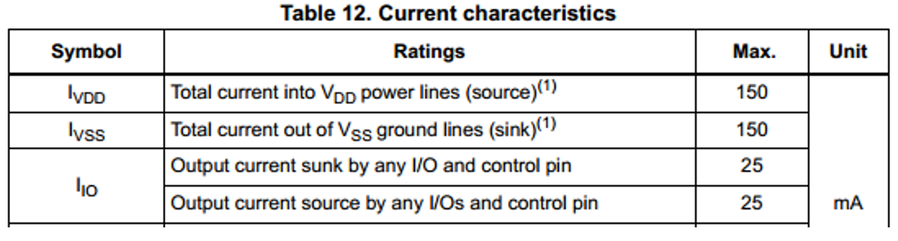
Figure 4‑2: Table shows the maximum driveable current from STM32F4DISCOVERY
(STMicroelectronics, DS8626: STM32 F407xx Datasheet-production data [Online], 2013, p. 77)
5 References
(STMicroelectronics, DS8626: STM32 F407xx Datasheet-production data [Online], 2013) STMicroelectronics. (2013, Jun). STM32F407xx Product-Specifications [Online]. Available: http://www.st.com/web/en/resource/technical/document/datasheet/DM00037051.pdf
[2] STMicroelectronics. (2013, Jun). STM32F417xx Datasheet – production data [Online]. Available: http://www.st.com/st-web-ui/static/active/en/resource/technical/document/datasheet/DM00035129.pdf
[3] STMicroelectronics. (2013, Feb). RM0090: STM32F40xxx Reference Manual [Online]. Available: http://www.st.com/st-web-ui/static/active/en/resource/technical/document/reference_manual/DM00031020.pdf
Saadi, M., L. Wattisuttikulkij, Y. Zhao, and P. Sangwongngam. “Visible light communication: opportunities, challenges and channel models.” International Journal of Electronics & Informatics 2, no. 1 (2013). Available: http://www.cennser.org/IJEI/eiV02N01/ei020101.pdf