How to Use Internal Flash Memory
download all demo files: Flash.7z
1 Internal Flash Memory
1.1 Introduction
In embedded systems, it is very important to have a memory which can store the information. Programs (set of instructions) are used to make an embedded system behave in such a manner according to the user requirements. Our programs are written in C or Waijung Blockset which compiles the set of instructions. Microcontroller uses flash memory which can be erased and re-programmed. Some space of the memory can be re-programmed and some space of the memory is fixed (i.e. cannot be re-programmed) and it depends on the manufacturer of the microcontroller how they manages the memory allocations.
STM32F4DISCOVERY board have a STM32F407VGT6 microcontroller which has a capacity of 1 MByte flash memory. The flash memory of the microcontroller has been divided into the sectors and each sector have its respective starting and ending addresses. Some sectors are of small size and some are of large size. Allocation of flash memory space is shown in Figure 1‑1.
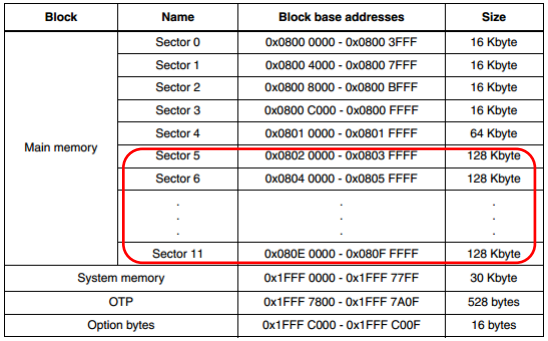
Figure 1-1: Allocation of flash memory space within the STM32F407 [1, p. 54]
The allocation of internal flash memory of STM32F407 is as follows.
- Main memory is divided into 11 sectors. First fours sectors (0-3) are of 16 KB, next sector is of 64 KB and remaining 5 sectors are of 128KB each;
- System memory is boot-loader;
- 512 KB memory is the write once memory and is used for general purpose. 16 more bytes are used for data lock;
- Option bytes are used for setting the Read/Write protection, Brown reset (to detect the power supply), the hardware/software watchdog etc.
The Waijung library has a blockset for using Internal Flash Memory Block having an option of erasing read and write data. The use is limited from sector 5 to 11.
1.2 How to use Flash Memory Block
Simulink library >> Waijung Blockset >> STM32F4 target >> On Peripheral Chip >> FLASH contains a blockset for managing the data in the flash memory. Flash Erase block parameters are shown in Figure 1‑2 which is used for deleting the data from the sectors. It takes about 1 to 2 seconds to erase the data from 128 KB memory [2, p. 106].
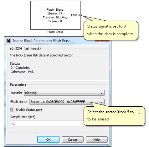
Figure 1-2: Features of Flash Erase Block
Block parameters of Flash Read are shown in Figure 1‑3. It is used to read the data from specified memory. For example, if used wants to read the address: 0x080E0500, following are the steps.
- From the required address, select the correct sector. The address: 0x080E0500 is in Sector 11
- For finding the Offset = Required Address – First Address in the Sector
Thus Offset = 0x80E0500 – 0x80E0000
= 0x0000500 = 20480 (in decimal)

Figure 1-3: Characteristics of Flash Read Block
Flash Write block is shown in Figure 1-4. It is used for write data to the memory offset of specific sector id. The procedure for assigning the address and specifying the offset address is same as that of Flash Read Block as described above.
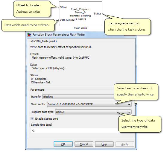
Figure 1-4: Characteristics of Flash Back Block
2 Testing the Flash Memory
2.1 Equipment used in the Experiment
- aMG F4 Connect board with a set of DIP switch, 2 push button switches and a If users doesn’t has aMG F4 Connect board then they can connect with these push button switch circuit, DIP switch circuit, LED circuit.
- STM32 Link Utility software which can be downloaded from the following website
http://www.st.com/web/catalog/tools/FM146/CL1984/SC724/SS1677/PF251168.
2.2 Experiment for Saving and Deleting Data
Objective
- Enable the users to understand the process of saving the data into the flash memory;
- Enable the users to understand the process of deleting the data from flash memory;
- Enable the users to observe the changes to the data in the STM32 ST-Link Utility memory program.
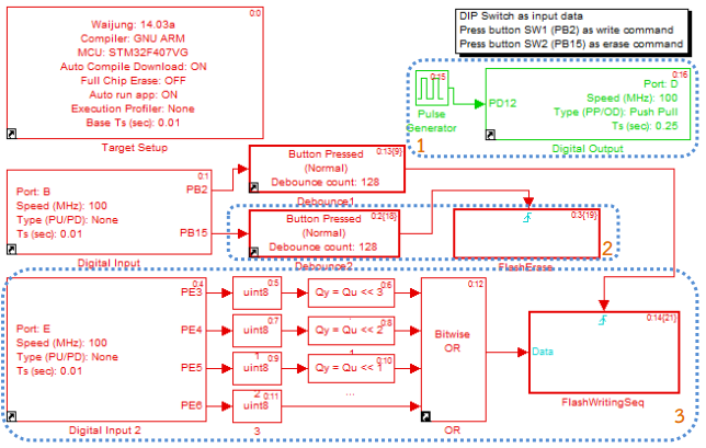
Figure 2-1: Simulink model for writing and erasing the data from flash memory
This experiment is conducted to write or erase flash memory address at 0x080E0500 using Simulink model as shown in Figure 1‑1 which consists of a three major blocks.
- First block is responsible for noting what user wants i.e. either user wants to write data to the memory or wants to erase data from the memory. This is governed by observing the position of SW1 and SW2.
- The signal from SW2 is connected to pin PB15 to erase the contents of internal flash memory. Flash Erase subsystem model is shown in Figure 2‑2. To delete the data from a sector, user need to select the respective sector of Flash Erase Block.
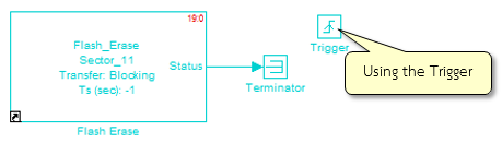
Figure 2-2: Within Flash Erase Subsystem model
- The signal from the switch SW1 is connected to pin PB2 to save the information at 0x080E0500 address. The user can set or adjust the DIP switch, the input will be converted to 8-bit integer and sent to the subsystem as shown in Figure 2‑3.
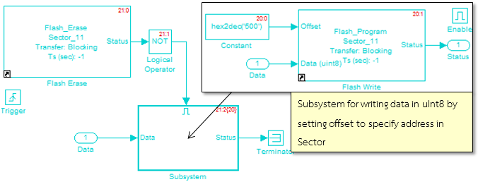
Figure 2-3: Within FlashWritingSeq Subsystem model
While writing in the flash memory, it is good to erase the already existing information on that sector which can be done by using Flash Erase Block which will delete the information of the entire sector.
After the Simulink model is downloaded into STM32F4DISCOVERY board, LED1 which is connected with PD12 will blink. To observe the changes in the flash memory, this experiment uses STM32 ST-Utility program and have the following main steps.
2.2.1 Procedure for Connecting STM32 ST-Utility
- Click on STM32 ST-Utility icon to open the program and then select Connect to Target. The ST-Link Utility will start the connection.

Figure 2-4: STM32 ST-Link Utility window after connecting with STM32F4DISCOVERY
- When successfully connected, then the device ID and flash memory size will appear on the terminal of the ST-Link Utility as shown in Figure 2‑4. LED (LD1) on STM32F4DISCOVERY will start flashing and initially the board will be in halt condition.
- Select Manu >> Target >> MCU Core from the core panel as shown in Figure 2‑5. Click on Run button and for the given example LED1 will start flashing.
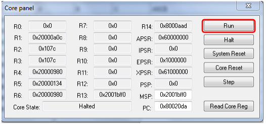
Figure 2-5: Core panel window
- Disable Live Update by unchecking the check box under Device Information.
- If user wants to download a new Simulink model into the device, user must select Disconnect icon every time before downloading the model.
2.2.2 How to use Memory Display
Data in memory will be shown in hexadecimal format in a table form. Rows and columns show the position of address. User can adjust the memory display as follows.
- Set the first position of the address. For example, setting 0x0800E000 data in that address will be at upper left position as in Figure 2‑6.
- Size address is used for setting the number of all addresses to be displayed in the table.
- Adjust data width to see data in 8 bits (1 byte), 16 bits (2 bytes) or 32 bits (4 bytes).
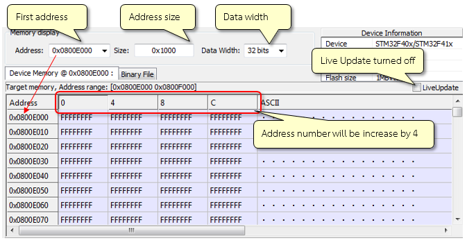
Figure 2-6: Window displaying data in the memory (Data Width 32 bits or 4 Bytes)
When user set the Data Width = 8 bits on the memory display then the display will change as shown in Figure 2‑7. Now the size of address is 8 bits value (00 to FF).
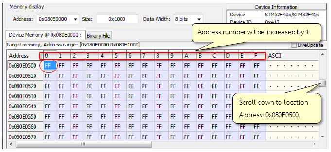
Figure 2-7: Window displaying data in memory (Data Width 8 bits or 1 Byte)
2.2.3 Experiment with Writing and Erasing
- Users can adjust the DIP switch from 1 to 4 positions i.e. ON-ON-OFF-OFF
- Press and hold SW1 switch for 1 second (Debounce count: 128). LED1 will blink while data is erased and written.
- Press LiveUpdate to see the value in the 0x080E0500 address as shown in Figure 2‑8.
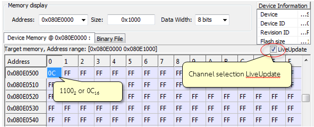
Figure 2-8: Windows displaying the data in memory after writing
- If user wants to edit data, turn off the LiveUpdate then do step 2 and 3 again.
- Press SW2 switch for 1 second to erase sector 11 (disable LiveUpdate for all the editing in Flash memory)
- Repeat step 3 for more information. The results shown in Figure 2‑9 tells that’s the value of the memory address 0x080E500 is equal to FF.

Figure 2-9: Window displaying the data in memory after deletion
2.3 Experimental data from Flash Memory
Objective
- To enable users to read data from a Flash Memory using Flash Read Block.
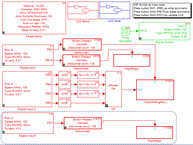
Figure 2-10: Simulink Model for reading data from Flash Memory and displayed through the LCD
From the example, in this experiment, users can observe data by STM32 ST-Utility connected to a computer with USB cable. Furthermore, user can observe data that has been record via LCD.
This experiment uses the model as shown in Figure 2‑10 for reading data from the flash memory and display it on the LCD which is an additional part when compared with the model shown in Figure 2‑1. Switch SW3 is used for updating the value read from flash memory and then display it on LCD. Figure 2‑11 shows internal subsystem model for reading data at address: 0x080E0500.
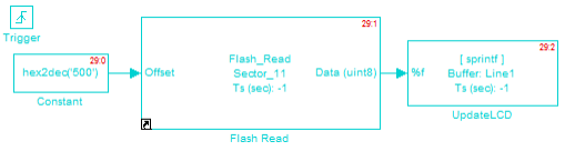
Figure 2-11: FlashRead Subsystem Model for reading data from Flash Memory
If user wants to write multiple data sets, user can edit Block in FlashWriteSeq Subsystem as in Figure 2‑13. In this example, 3 sets of data are written which have different type of variables (uint8, uint32 and single). User can add Flash Write Block and set any address within range of 4 Bytes
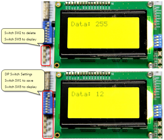
Figure 2-12: Values read from Flash Memory through the LCD display
If user wants to write multiple data sets, user can edit Block in FlashWriteSeq Subsystem as in Figure 2‑13. In this example, 3 sets of data are written which have different type of variables (uint8, uint32 and single). User can add Flash Write Block and set any address within range of 4 Bytes.
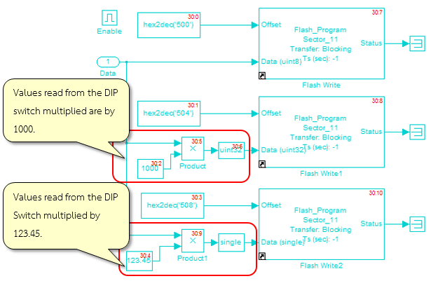
Figure 2-13: Subsystem model for writing or recording in multiple Flash Memory
So in the example, if the value read from the DIP switch is set to 12. Information address: 0x080E504 is equal to 12000 and address: 0x080E508 is equal to 1481.40 so users can check in flash memory window which displays the data in memory as shown in Figure 2‑14.
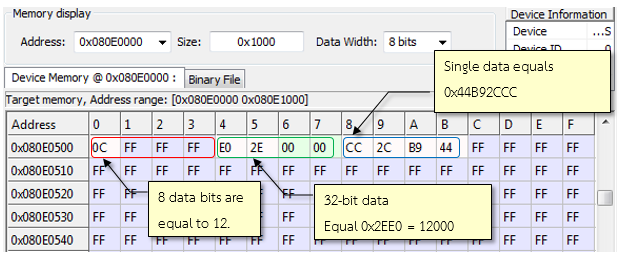
Figure 2-14: Window displaying data in the memory
Users can learn how to convert a decimal number to binary floating-point arithmetic from the following link http://www.h-schmidt.net/FloatConverter/IEEE754.html. This is known as IEEE-754 standard.
Figure 2‑15 is an example of subsystem for reading 3 data sets of different type of variables (uint8, uint32 and single). User can add the Flash Read Block and set address that want to read.
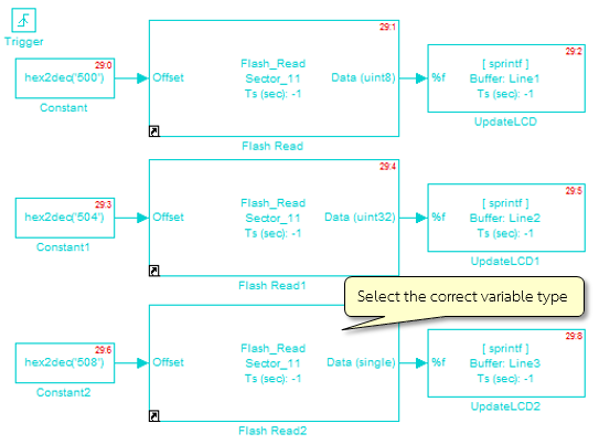
Figure 2-15: Subsystem for reading data of multiple types
Download the model and information stored in DIP switch, SW1 switch and SW2 switch will be displayed on the LCD display which is shown in Figure 2‑16.
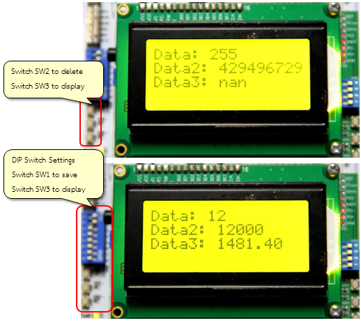
Figure 2-16: Reading value from multiple data sets of flash memory and display it on the LCD
Although user can turn ON-OFF the electric power or download model into STM32F4DISCOVERY again, data in sector 5 – sector 11 will still remain unchanged. So using internal flash memory is suitable for working with data which is not changed so often, for example security or setup section.
3 References
- STMicroelectronics, “RM0090: STM32F40xxx Reference Manual [Online],” 2013.
- STMicroelectronics, “STM32 F407xx Datasheet-production data [Online],” 2013.
- STMicroelectronics, “User manual: STM32 ST-LINK Utility software description [Online],” 2014.
- Olaf Pfeiffer and Andrew Ayre, “Using Flash Memory in Embedded Applications,” [Online]. Available: http://www.esacademy.com/en/library/technical-articles-and-documents/8051-programming/using-flash-memory-in-embedded-applications.html.
- IEEE, “IEEE Standard for Floating-Point Arithmetic”, 2008
- http://en.wikipedia.org/wiki/IEEE_754-1985