How to Use SPI Communication Port
download all demo files: SPI.7z
1 Using SPI Communication Port
1.1 Knowing SPI
Serial Peripheral Interface or SPI is another form of Serial Synchronous Communication. In this type of communication one device works as Master while another acts as a Salve. Master device initiates the data frame and there can be multiple slave devices. SPI works in full duplex mode. Signals between Master and Slave can be sent simultaneously. One of the biggest advantage of SPI protocol is that the complete protocol has flexibility for the bits transfer and not limited to 8-bit words. There can be arbitrary choice of message size content and purpose.
Here are few examples for the devices which uses SPI communication
- The module that converts analog signals to digital and vice versa;
- Communication with EEPROM and FLASH memory;
- Digital clock module with Real Time Clock (RTC);
- Temperature and pressure sensors;
- Other equipment such as signal mixer, potentiometer, LCD controller, USART, CAN controller, USB controller amplifier.
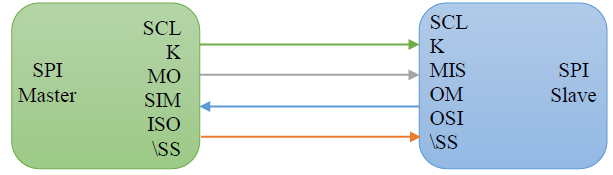
Figure 1‑1 shows the connection between SPI Master and Slave. The link have four lines/wires
- SCLK (Serial Clock) to the clock signal given from Master to the Slave device to set the tempo for data transmission;
- MOSI (Master Out Slave In) use data from device to device i.e. Master Slave;
- MISO (Master In Slave Out) is used to receive data from Slave;
- \SS (Slave Select) pin or CS (Chip Select) transmit low signal to the desired Slave devices with which it want to exchange data.
Master device’s function is to control all communications with clock signal and signal line SS. The Master will decide whether to receive or send data into slave device signal line SS (Slave Select) in case of having more than one slave by make signal level of that SS LOW. If we want to connect to particular SS, just set the signal level of that SS to LOW as shown in Figure 1‑2.

Figure 1-2: SPI communication between Master and Slave
When comparing the SPI communication with I2C communication, the former one has higher throughput and is ideal for low speed data communications such as EEPROM memory module or digital clock.
SPI communication has an advantage of full duplex communication that is able to transmit and receive simultaneously for particular cable. Typically SPI has lower power requirements than I2C due to simple hardware interface. Slaves use the master’s clock and do not require precision oscillators. SPI is not limited to any maximum clock speed, enabling potentially high throughput.
1.2 Using SPI Blockset
Waijung Blockset consists of SPI Master Setup Block as shown in Figure 1‑3. To set any Register values related to SPI communications i.e. select SPI module in STM32F4DISCOVERY up to three sets, select pin MOSI/MISO/SS and set frequency of clock signal in SCLK.
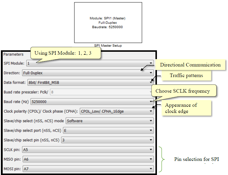
Figure 1-3: Characteristics of settings of SPI Master Setup Block
SPI communication has no certain pattern, in order to set communication pattern of Master device to match with Slave we have to do the following things:
- Set communication direction, Full Duplex (receive and transmit data in same time) Half Duplex Tx (transmission only), Half Duplex Rx (receive only)
- Data receiving and sending format 8 or 16 bit, can select first bit to send either most significant bit (MSB) or lowest significant bit (LSB)
- Form of clock signal edge to setting tempo of receiving – sending data. There are 4 types:

Figure 1-4: Data is received or sent when CPOL = 0 and CPHA = 0 0 [1, p. 800]
When the clock polarity is LOW and clock phase 2nd edge (CPOL_Low/CPHA_2Edge), the system will start reading first bit when found second edge of signal (negative edge) as shown in Figure 1‑5.
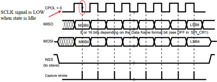
Figure 1-5: Data receiving and sending when CPOL = 0 and CPHA = 1 [1, p. 800]
When the clock polarity is HIGH and clock phase 1st edge (CPOL_High/CPHA_1Edge) is at the initial state (clock signal will be in HIGH state), the system will start reading first bit when found first edge of signal (negative edge) as shown in Figure 1‑6
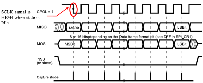
Figure 1-6: Data receiving and sending when CPOL = 1 and CPHA = 0 [1, p. 800]
When the clock polarity is HIGH and Clock phase 2st edge (CPOL_High/CPHA_2Edge), the system will start reading first bit when found second edge of signal (positive edge) as Figure 1‑7
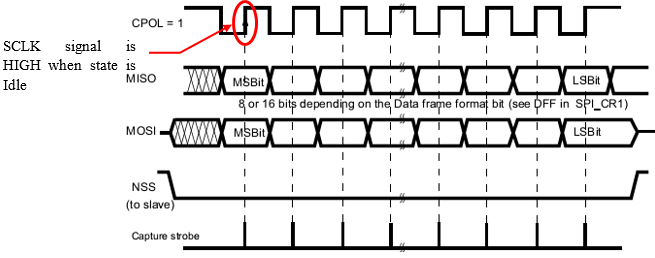
Figure 1-7: Data receiving and sending when CPOL = 1 and CPHA = 1 0 [1, p. 800]
SPI Master Read/Write Block as shown in Figure 1‑8 receives or sends data into slave device by SPI. STM32F4DISCOVERY is used as Master device and user can set number of byte which need to be sent.
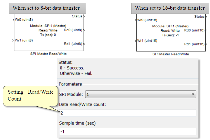
Figure 1-8: Properties and setting the values of SPI Master Read/Write Block
2 Example of using DAC with SPI communication
This section describes how to use SPI communication to control devices. This example given below uses IC LTC1661 (from Linear Technology). Signal converter module is used to convert 10 bits to 2 analog channels. Although STM32F4DISCOVERY has 2 DAC channels, users can use this device if they want to add more analog voltage supply channel.
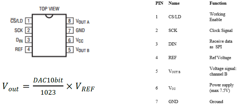
Figure 2-1: IC PINs of LTC1661 [2]
Figure 2‑2 shows the data of LTC1661 through SPI to adjust the voltage. When looking at clock signal pattern, in Idle state, the signal is LOW and reads data bit on MOSI when the positive edge is found (1st edge capture). One data set has 16 bits containing a digital value. 10 bits are needed to convert the voltage value and 4 bits control code for controlling IC LTC1661 and last two bits are don’t care bits as shown in Figure 2‑3. Maximum frequency of clock signal that IC LTC1661 can work properly is 16.7 MHz [2, p. 3].
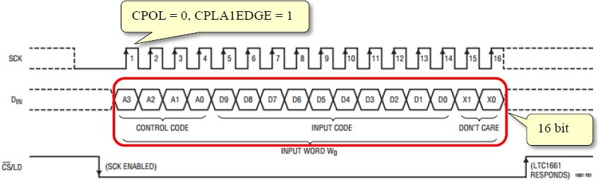
Figure 2-2: SPI Communication of IC LTC1661 [2, p. 9]
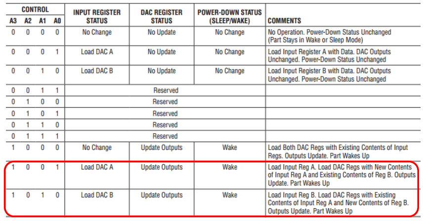
Figure 2-3: Description table of Control Code of IC LTC1661 [2, p. 9]
2.1 Experiment Devices
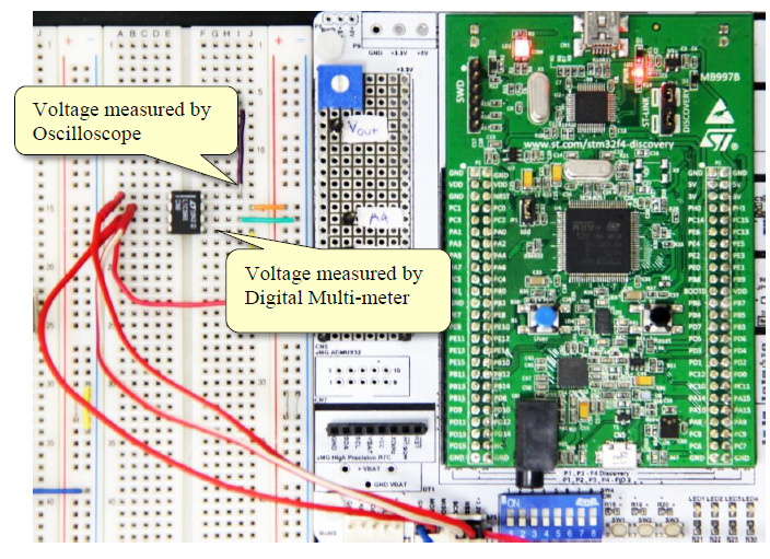
Figure 2-4: Installation of signal generator with IC LTC1661
Figure 2‑4 shows connection between STM32F4DISCOVERY and IC LTC1661 on the aMG F4 Connect board having port to connect SPI device by setting PA15 pin as Slave Select (NSS), PB3 pin as SCLK, PB4 pin as MISO and PB5 pin as MOSI. IC LTC1661 receives data from Master device only. Users just have to connect transmission line for MOSI data.
Table 2-1: Connection between STM32F4DISCOVERY and IC LTC1661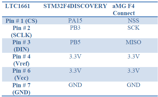
2.2 Experiment to Use IC LTC 1661 on SPI Communication
Objective:
- User can setup and configure SPI for each device;
- User can generate electric voltage by IC LTC 1661.
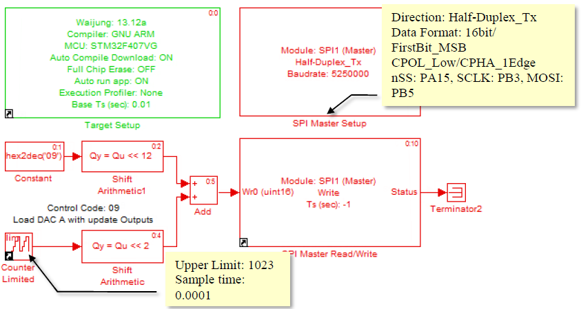
Figure 2-5: Simulink Model to generate one channel analog signal with ICLTC1661
Figure 2‑5 shows Simulink model for creating one channel analog signal with IC LTC1661 through SPI communication. After downloading the model into STM32F4DISCOVERY, the value of Control Code = 1001 and value from Counter Limited Block will be exported and Counter Limited Block will start counting from 0 to 1023 every 0.1 ms to Slave device for DAC. After 0.1 second, the value of Counter will start from 0 again (So the signal frequency is 10 Hz). Figure 2‑6 shows the signal measured from pin 8 (Vout A) of IC LTC1661 using Oscilloscope.
The measurements from Figure 2‑6 shows the signal frequency of 9.766 Hz or has signal period = 0.102 seconds and maximum signal value is around 3.04 V.
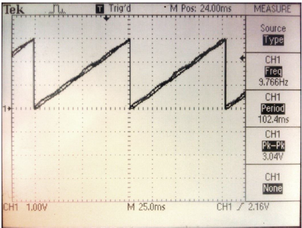
Figure 2-6: Experiment result of analog signal generation with IC LTC1661
Figure 2‑7 shows a Simulink Model for constructing two channels of analog signal. Control Code = 10 is used for sending DAC to B channel, and Pulse Generator Block is used for selecting data to send to SPI.
When the value of Pulse Generator Block is 0 and the value of Control Code = 1010, a constant value of 256 will be sent thus VoutB = (259 / 1023) x 3 = 0.826V (can measure by Digital Multimeter). When Pulse Generator Block = 1 and value of Control Code = 1010 and value of Counter will be sent alternatively every 0.05 ms.
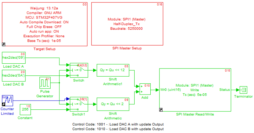
Figure 2-7: Simulink Model to generate two channels analog signal with multiplexer technique
3 Reading the Value of Linear Accelerometer LIS302DL
Nowadays, the use of linear accelerometer has been increased tremendously in smart control systems such as screen adjustment of LCD in smartphones and notebooks, vibration detector, burglar alarm and subsystem of navigational system in unmanned aerial vehicle (UAV).
When we are on earth surface and drop an object to the earth, that object will fall into the ground with constant acceleration known gravitational acceleration (g). The value of g is known to be 9.8 m/s. If we measure an object with 3g acceleration, it means it is travelling with the speed three times than the gravitational acceleration.
3.1 Experiment Devices
This experiment uses STM32F4DISCOVERY as shown in Figure 3‑1 installed with accelerometer LIS302DL developed by STMicroelectronics. Properties of LIS302DL are:
- Acceleration measuring in X, Y, Z;
- Selectable full scales of ±2g or ±8g;
- Send the measured value via serial communication I2C or SPI;
- Selectable transmission rate 100Hz or

Figure 3-1: Device installation for reading data from LIS302DL sensor through SPI communication
In order to read data from SPI, user need to read the communication format of LIS302DL from Datasheet [3]. Data reading formats of LIS302DL has two ways to read, one byte (8 bits data) and multiple bytes per time. Number of bytes depends on command. Figure 3‑2 shows the data format of LIS302DL. Master device send the command and address of internal register of LIS302DL.

Figure 3-2: Data reading form of LIS302DL through SPI 1 byte per time [3, p. 22]
Multiple bytes reading can be done by setting M/S = 1 and define the initial start address. Data from LIS302DL will be sent to Master device on the tempo of SCLK signal. When 8 bits are sent already, LIS302DL will send data from next address until the Master device stop data reception.

Figure 3-3: Data reading form of LIS302DL through SPI, multiple bytes (in this example 2 bytes)
Writing data into LIS302DL has two ways too. In Figure 3‑4 and Figure 3‑5 shows data writing to LIS302DL one byte and multiple bytes per time respectively. Master device send writing command and address of internal register of LIS302DL then data is sent to set value in that register.
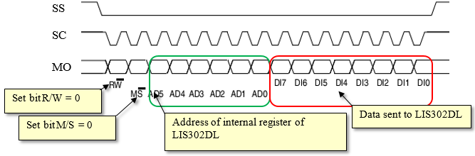
Figure 3-4: Data writing form of LIS302DL through SPI one byte per time [3, p. 22]
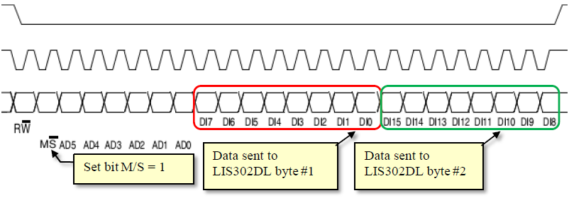
Figure 3-5: Data writing form of LIS302DL through SPI multiple bytes [3, p. 23]
Figure 3‑6 shows the address of internal register of LIS302DL. Each register has different functions, such as controlling the functionality of the sensor, store variable values and store the measured linear acceleration value etc.

Figure 3 6: Address of internal register of LIS302DL [3, p. 24]
Simulink model for reading acceleration values in three axis of LIS302DL sensor is shown in Figure 3‑7. The model in figure below has three main functions:
- LIS302DL initialize subsystem for setting initial value;
- LIS302DL read subsystem for reading acceleration value in axis X, Y and Z;
- UART Tx is for sending acceleration value using UART Tx communication.
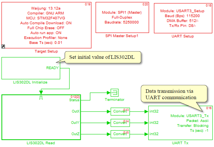
Figure 3-7: Simulink Model for reading data from LIS302DL sensor through SPI communication
After downloading model into STM32F4DISCOVERY, the program will read initial state of LIS302DL by subsystem as in Figure 3 8. That is the one byte data reading as SPI from CTRL_REG Register at (Address 0x20). If the read value is not equal to 0xC7, the data is written as SPI at CTRL_REG Register.
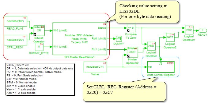
Figure 3-8: Subsystem model for setting up initial value of LIS302DL
Then LIS302DL Read Subsystem starts to read the acceleration values of the three axis. All data are in Out_X, Out_Y and Out_Z Register (Address 0x29, 0x2A and 0x2D) respectively. Figure 3‑9 shows data reading as SPI 6 bytes and set Out_X to be starting address.
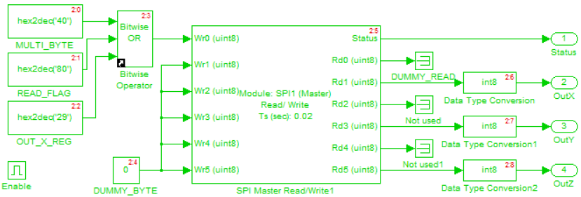
Figure 3-9: Subsystem Model for reading acceleration value of three axes from LIS302DL
The read value is int8 type, signed integer 8 bit (value -127 to 127) and display it via UART communication every 0.02 seconds or 50 Hz. Figure 3‑8 shows settings of Full Scale selection (FS) = 0. That’s means measuring linear acceleration in interval ±2g thus linear acceleration (unit: g m/s2) can be calculated from equation:Then LIS302DL Read Subsystem starts to read the acceleration values of the three axis. All data are in Out_X, Out_Y and Out_Z Register (Address 0x29, 0x2A and 0x2D) respectively. Figure 3‑9 shows data reading as SPI 6 bytes and set Out_X to be starting address.
Acceleration = 2 x measured value/ 127
When the Z-Axis of sensor is in the line of the gravity, the measured acceleration is 1g or the value = 64
Figure 3‑10 shows linear acceleration via TeraTerm program on STM32F4DISCOVERY. Acceleration value in Z-axis will be maximum because of gravitational acceleration and the value in X-Y axis will be minimum because they are parallel with earth surface.
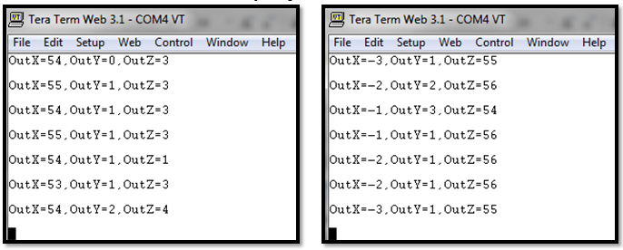
Figure 3-10: Experimental results of linear acceleration data reading
3.2 Example of Acceleration Detection in case of Crash.
When an object is crashed, the acceleration will be changed in short time and we can use the sensor to detect it and bring that value to alarm or control any devices for further processing. For the examples, burglar alarm, vibration detector, safety airbag, etc.
Figure 3‑11 shows Simulink model to display the value of linear acceleration in real time. This model is working on computer (Don’t need to download into STM32F4DISCOVERY) when connected STM32F4DISCOVERY via USB and press Run icon. This program will read linear acceleration value from STM32F4DISCOVERY through USB cable.
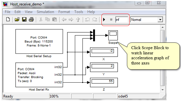
Figure 3‑11: Simulink model to display result of linear acceleration in real time
Note: You should close all serial communication programs before running this model.
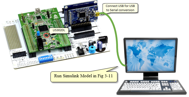
Figure 3-12: Devices preparation for experimenting with linear acceleration in real time
After double clicking the Scope Block, graph of linear acceleration in 3 axis will appear in real time, it mean the pattern of graph will change if STM32F4DISCOVERY changes its position as in Figure 3‑13.
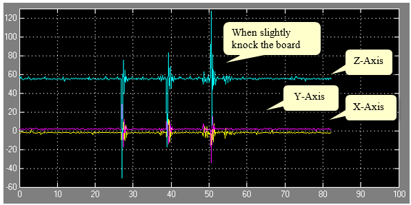
Figure 3‑13: Graph of real time linear acceleration measured by LIS302DL
4. References
- STMicroelectronics, “RM0090: STM32F40xxx Reference Manual [Online],” 2013.
- STMicroelectronic, “LIS302DL MEM motion sensor,” 2008.
- Linear Technology, “LTC1661 Micropower Dual 10-Bit DAC in MSOP,” 1999.
- K. a. R. Kalinsky, “Introduction to Serial Peripheral Interface,” Embedded.com, UBM Electronics, 2002. [Online]. Available: http://www.embedded.com/electronics-blogs/beginner-s-corner/4023908/Introduction-to-Serial-Peripheral-Interface.
- P., “การติดต่อสื่อสารด้วย SPI : Serial Peripheral Interface,” [Online]. Available: http://www.123microcontroller.com/Hardware-Interfacing/SPI-Serial-Peripheral-Interface-communication. [Accessed 27 February 2014].